2024-11-14
-ALINX NVMe IP-
In the current data-driven era, the demand for high-performance storage solutions for enterprises continues to grow. NVMe AXI IP has become an ideal choice for many developers and enterprises due to its storage performance advantages such as support for large data volumes, high-speed transfers, and low latency.
Built specifically for SSDs, NVMe delivers significant performance gains, especially in random I/O operations, by directly utilizing the PCIe channel and avoiding the additional latency of the SATA protocol and external controller (PCH).
NVMe PCIe SSDs deliver up to ten times the IOPs of high-end enterprise SATA SSDs (in scenarios such as random reads and writes with high queue depths), and support automatic power state switching and dynamic energy management features to significantly reduce power consumption.
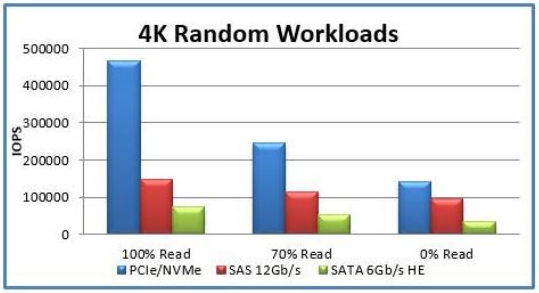
( NVMe/SAS/SATA Storage Device Read Performance Comparison)
With its high-speed transmission, low latency, high-performance storage, and high reliability, the NVMe protocol is widely used in data centers, edge computing, enterprise storage, AI servers, and cloud computing.
ALINX NVMe IP Details
ALINX NVMe IP is deeply optimized for today's data-intensive applications, significantly reducing latency and increasing data throughput to meet the urgent needs of cutting-edge fields such as cloud computing, big data analytics, AI, and virtual reality/augmented reality (VR/AR).
In terms of compatibility, NVMe IP does not rely on the CPU, but is processed by the FPGA, which requires sufficient resources and appropriate hardware support. ALINX NVMe IP currently supports AMD Virtex 7/ AMD UltraScale/ AMD UltraScale+ series devices.
In terms of technical support, ALINX provides comprehensive technical support and efficient customization services, with an experienced IP R&D team dedicated to assisting customers with IP integration and performance optimization to ensure that customer needs are realized quickly.
Considering that each application scenario has its own unique requirements, ALINX NVMe AXI IP provides developers with a wealth of customization options, allowing precise tuning of its performance based on specific application requirements, including but not limited to optimizing data transfer rates under specific workloads, configuring it for different storage capacity needs, and so on.
Below is a detailed description of ALINX NVMe IP:
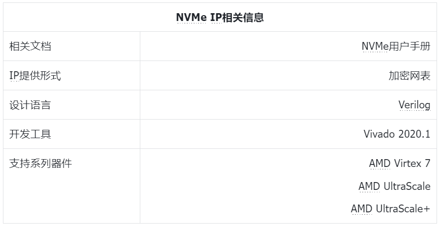
IP Resource Consumption Table

Note: IP actual logical resource consumption is affected by other logical resource consumption in instantiation
Product Features
· Function Support: Command support (Identify, Write, Read, Flush), compatible with NVMe 1.4 protocol, supports PCIe Gen 1.0-4.0;
· Performance Parameters: (1) Maximum Queue Depth: Supports 65535 I/O commands per queue; (2) Transfer Rate: Based on PCIe 3.0 X4, both read and write rates up to 3000MB/s;
· Flexibility: Supports multiple storage units (512 bytes / 4096 bytes);
· Support for customization services: including data transfer rate optimization and storage capacity configuration;
· Version support: supports two versions (AXI FULL version / AXI Stream version);
· Reference design: XCZU19EG + FMC daughter board (FH1402) + SAMSUNG 980 M.2 SSD.
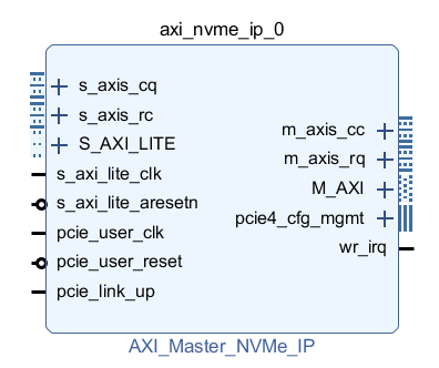
· AXI-Master-FULL version
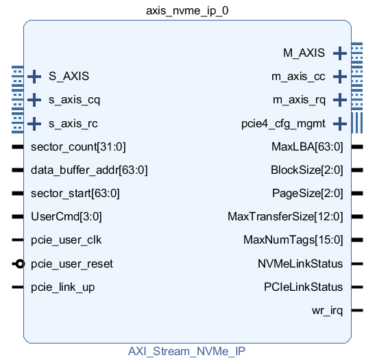
· AXI-Stream version
NVMe AXI IP Application Interaction
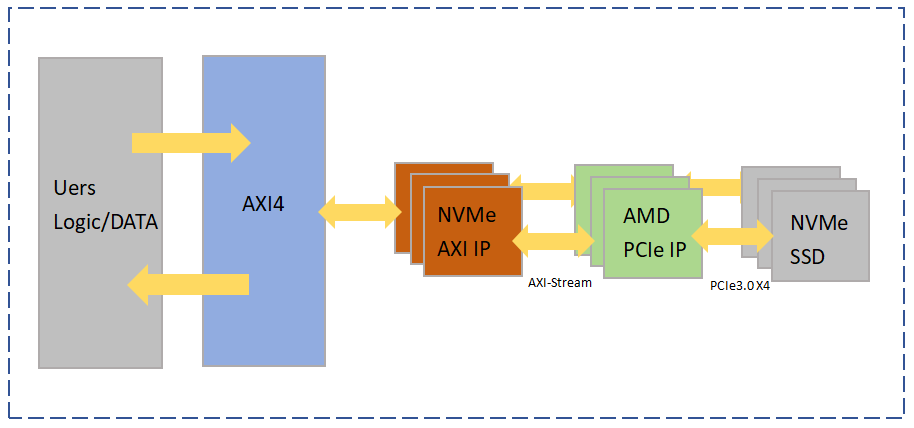
NVMe AXI IP realizes PCIe protocol interaction through PCIe Bridge, supporting two interface modes: AXI FULL and AXI Stream. After user data is accessed through AXI Interconnect, it is processed by the protocol logic of NVMe AXI IP, packaged into PCIe TLP packets, and written to NVMe SSD storage; similarly, after the data is extracted from the NVMe SSD, it is passed to the upper logic through the protocol parsing and AXI interface.
Example
· AXI-Master-FULL version
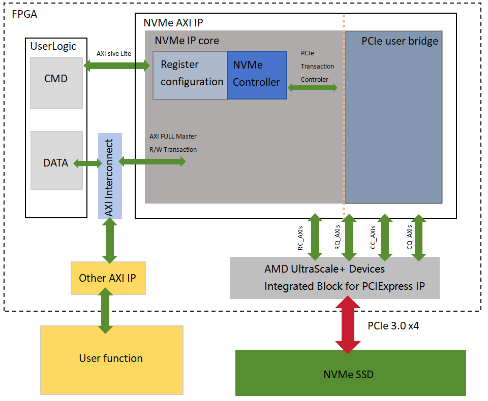
AXI Read/Write: After normal system startup, the NVMe AXI IP automatically initializes and establishes the PCIe link connection. After the initialization is completed, the user's data stream is transmitted through the AXI Interconnect IP to the AXI Master FULL interface of the NVMe AXI IP for NVMe protocol processing. The data is packetized into TLP layer PCIe packets and connected to the AMD UltraScale+ device's PCIe Integrated Block for PCIExpress via the RC/RQ/CC/CQ AXI Stream interface, and ultimately written to NVMe SSD storage. When it is time to read data, the NVMe AXI IP extracts the data from the NVMe SSD via the RC/RQ/CC/CQ AXI Stream interface and connects to the AXI Interconnect IP via the AXI Master FULL interface to transfer the data to the other AXI bus interfaces for use by user logic.
· AXI-Stream version
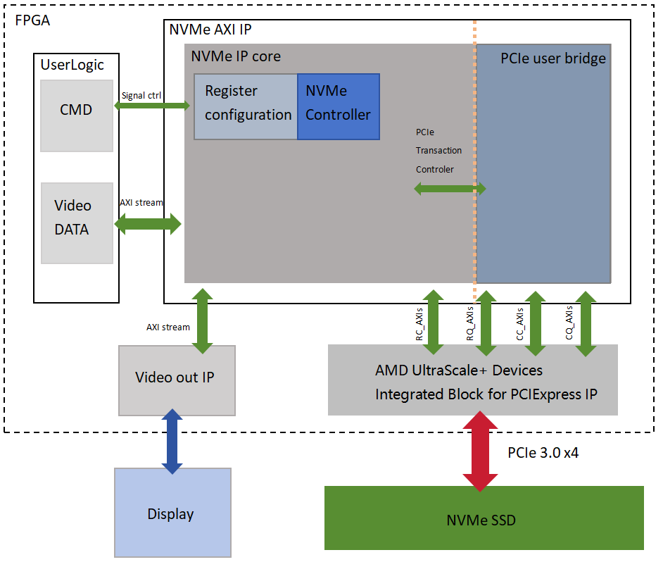
AXI Stream Read/Write: After normal system startup, the NVMe AXI IP automatically initializes and establishes a connection. After the initialization is completed, the user's data stream is input to the NVMe AXI IP through the AXI Stream interface to perform the interactive processing of the NVMe protocol. The data is packaged into TLP-layer PCIe packets, connected to the AMD UltraScale+ device's PCIe integration module via the RC/RQ/CC/CQ AXI Stream interface, and ultimately stored on the NVMe SSD. when reading from the NVMe SSD, the NVMe AXI IP uses the RC/RQ/CC/CQ AXI Stream interface to extract the data and store it on the NVMe SSD via the AXI Stream interface. When data is read from the NVMe SSD, the NVMe AXI IP uses the RC/RQ/CC/CQ AXI Stream interface to extract the data and transmit it through the AXI Stream interface to the connected Video Output IP, which then displays the data through the video interface.